
HDI printed circuit board
A HDI printed circuit board is a multi-layered device used to house electronic components. Its specialized processes and unique constructions allow it to achieve much higher pin count densities than traditional PCBs without sacrificing performance. This means more features can be added to the PCB, including the ability to carry faster signals and more complex functions. In turn, this allows for sleeker designs that can be incorporated into the latest technological devices.
The manufacturing process of an HDI PCB requires a significant amount of time and special equipment. This includes laser drill technology to create the small micovias, a sequential lamination structure, and copper plating that is either electroless or electrolytic. The process also involves using thinner specialty materials. Consequently, HDI PCBs are more expensive to produce than traditional PCBs.
While the cost of an hdi printed circuit board is higher, it can offer several advantages to designers and manufacturers. These include: Due to the shorter trace widths, HDI PCBs can transmit signals with a lower impedance and lower power requirements than conventional boards. The use of buried vias and blind vias also reduces the overall board space, further improving signal integrity.
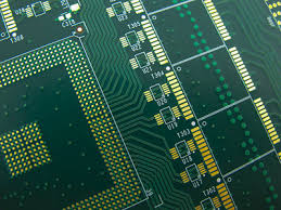
What is an HDI printed circuit board?
This technology is especially useful in medical applications where size and efficiency are essential. For example, implantable devices like pacemakers must be small enough to fit in the body, but still allow for high-speed transmission of signals. HDI PCBs make this possible, allowing for sleeker devices that can be more easily implanted into patients.
The HDI technology has also been instrumental in the miniaturization of electronic devices, such as smartphones, digital cameras, and touch-screen devices. The smaller components and routing structures of HDI PCBs can also accommodate larger amounts of data and higher pin counts. This has led to the creation of a wide range of new, innovative technologies that consumers can enjoy.
The increased packing density of HDI PCBs can help to increase the reliability of the final product. This is because the shorter track lengths and Microvias reduce the distance that signals have to travel between layers, minimizing cross-over delays and signal loss.
High-Density Interconnect (HDI) printed circuit boards (PCBs) represent a significant advancement in the world of electronics, offering enhanced performance, miniaturization, and functionality for a wide range of applications. HDI PCBs are characterized by their higher wiring density per unit area compared to traditional PCBs. This is achieved through the use of microvias, finer lines and spaces, and a higher level of interconnection layers, making them ideal for complex and compact electronic devices.
In addition, the lowered thickness of HDI PCBs can provide additional mechanical protection for sensitive components like sensors and actuators. This can prevent damage from shock and vibration, extending the lifespan of the device.
In order to get started with HDI PCBs, design engineers should consult with a reliable supplier that offers comprehensive assembly services. Sierra Circuits provides this and more, utilizing expert engineering and rigorous testing to deliver full turnkey circuit boards guaranteed to work. Contact us today to learn more about our capabilities and how we can help you meet your production needs.
