
Pcb productions support high-speed data transfer
In today’s fast-paced technological landscape, high-speed data transfer is a critical requirement for many electronic devices. As the demand for faster and more efficient communication between components grows, the role of PCB production becomes increasingly important. A printed circuit board (PCB) is the foundation on which electronic circuits are built, and its design directly affects the performance of high-speed data transfer. The question arises: can PCB productions support high-speed data transfer, and if so, how can they be optimized for this purpose?
High-speed data transfer refers to the rapid transmission of data between components on a PCB, such as processors, memory chips, and communication interfaces. As data speeds increase, the challenges associated with managing signal integrity, minimizing noise, and preventing data loss become more pronounced. High-frequency signals, when transmitted over a PCB, are subject to various forms of interference, including crosstalk, reflection, and signal attenuation. These factors can severely impact the quality of the data transfer, leading to errors, slower speeds, and even complete communication failure.
For pcb production to support high-speed data transfer, the design must address these challenges and ensure that the signals can travel quickly and reliably between components. This involves implementing specialized design techniques and manufacturing processes to maintain signal integrity and reduce noise.
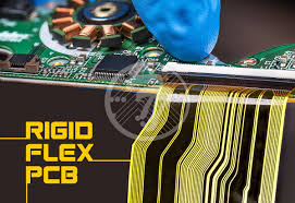
Can Pcb productions support high-speed data transfer?
One of the most critical factors in supporting high-speed data transfer in PCB production is maintaining controlled impedance. Impedance refers to the resistance of a signal as it travels through a transmission line, such as a PCB trace. If the impedance is not properly controlled, it can result in signal reflections, loss of data, or degraded signal quality. High-speed PCBs often use differential pairs (two traces carrying opposite signals) with tightly controlled impedance to ensure stable signal transmission.
High-speed signals can experience signal loss due to resistance, capacitive coupling, and inductance in the PCB traces. To minimize signal loss, PCB designers can use thicker copper traces, shorter trace lengths, and optimize the board layout to reduce resistance and inductance. Additionally, careful consideration of trace width, thickness, and spacing is essential to ensure minimal signal degradation over long distances.
In high-speed PCBs, the design of the layer stack-up and vias plays a significant role in minimizing interference and ensuring efficient data transfer. Multiple layers of copper can be used to create dedicated power and ground planes, which help to shield high-speed signal traces from noise. Proper via design is also essential, as poorly placed or improperly sized vias can introduce signal delays or unwanted reflections that degrade the quality of the data transfer.
Crosstalk occurs when signals from one trace interfere with those on adjacent traces, causing data corruption and reduced signal clarity. In high-speed PCB production, minimizing crosstalk is crucial. This can be achieved by increasing the spacing between signal traces, using ground planes to shield traces, and using differential pairs for high-speed signal transmission. Careful routing of traces can also prevent signal coupling and reduce the chances of crosstalk.
The materials used in PCB production also impact the ability of a PCB to support high-speed data transfer. Materials with low dielectric constants, such as high-frequency laminates, are often chosen for high-speed designs because they help to reduce signal loss and delay. These materials allow signals to travel faster with less attenuation, which is essential for maintaining data integrity at high speeds.
PCB production methods must be adapted to handle the specific needs of high-speed designs. The precision and quality of manufacturing processes such as etching, drilling, and plating are critical in ensuring the integrity of the PCB and its ability to support high-speed data transfer. Advanced techniques, such as laser drilling for precise via placement and high-precision etching for fine trace widths, are commonly used in high-speed PCB production. These processes help to maintain signal integrity and reduce unwanted impedance variations or losses.
